
MRAM (Magnetic Random Access Memory)
Memorizing “1” and “0” using magnetic polarity (magnetic information)
“High-speed, highly durable non-volatile memory”
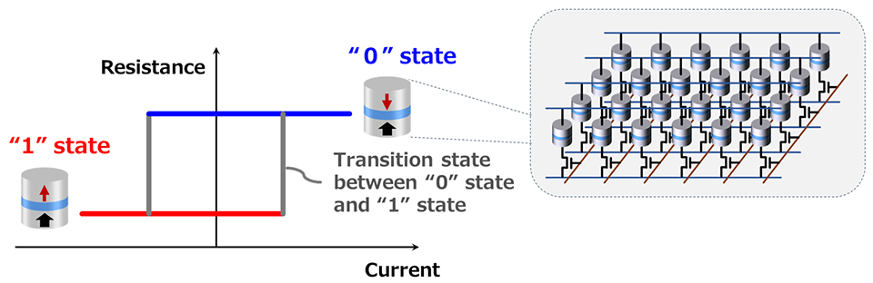
Magnetoresistive effect
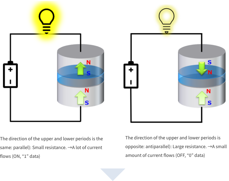
Memorizes “1” and “0” using magnetoresistive effect
Next generation memory overview
| DRAM | NAND | Next generation memory |
|
|---|---|---|---|
| speed | ○ (20nsec) |
× (10usec) |
○ (< 100nsec) |
| memory retention |
× (~msec) |
○ (A few years) |
○ (A few years) |
| durability | ○ (20nsec) |
× | ○ |
Excerpt from “Research and Development of Next Generation Memory” @P162 of Semiconductor/Digital Industrial Strategy (revised draft) @ June 2023
Advantages of MRAM
MRAM (Magnetoresistive Random Access Memory) is a nonvolatile memory that stores information in the direction of magnetization. High-speed operation is possible due to the high magnetization reversal speed of approximately 1 ns, and there is no atomic movement, making it highly resistant to rewriting, an advantage that other non-volatile memories do not have.
Basic element of MRAM: MTJ
Recent progress in MRAM technology began with a technological breakthrough by Professor Ohno’s group at Tohoku University in 2010. At the time, new materials for sandwiching insulators were being searched worldwide to improve device performance. In doing so, we discovered that by making conventional materials thinner, the electron spins (magnetic direction), which are normally horizontal to the substrate, become aligned perpendicular to the substrate at a certain thickness. As a result, the material has become a world standard material system, and full-scale commercialization began in 2018.
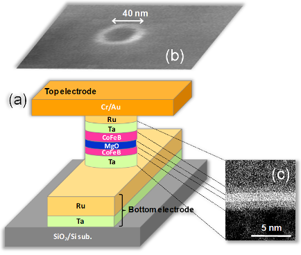
S. Ikeda,‥‥H. Ohno et al., Nature Materials 9, 721 (2010)
STT-MRAM
MRAM has different characteristics depending on the writing method. STT (Spin Transfer Torque)-MRAM has recently become widely used. The basic element of the STT-MRAM memory element is a two-terminal element with a three-layer structure called a magnetic tunneling junction (MTJ). “Reference layer”, “Tunneling layer” through which electrons pass through due to tunneling effect, and “Free layer” where the magnetization can be either parallel or antiparallel to the magnetization of the reference layer. Free Layer). With STT-MRAM, rewriting and reading can be achieved with one transistor (1Tr1MTJ), making it possible to reduce the memory cell area. Work is underway to replace the SRAM and embedded flash memory used in CPU cache memory, as well as stand-alone memory.
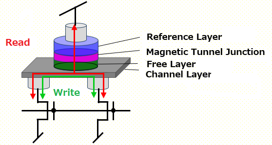
SOT-MRAM
Another promising next-generation technology is SOT (Spin Orbit Torque)-MRAM. A channel layer made of a nonmagnetic pure metal layer is formed in contact with the free layer of the MTJ element. Dedicated transistors are required for rewriting and reading (2Tr1MTJ), and the memory cell area is larger than STT-MRAM, but it can operate at higher speeds and achieve higher reliability. Research and development is underway with a view to replacing high-speed cache memory for HPC (High Performance Computing), such as AI processors.
| Architecture | STT-MRAM | SOT-MRAM |
|---|---|---|
| Structure | 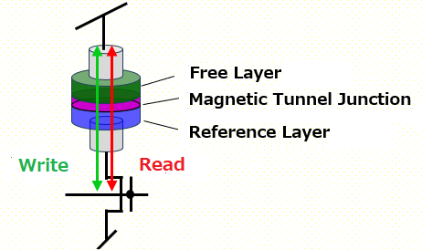 |
 |
| How to write | Spin Transfer Torque (STT) | Spin Orbit Torque (SOT) |
| Purpose | Large capacity | High speed |
STT-MRAM
- Structure
- How to write
- Spin Transfer Torque (STT)
- Purpose
- Large capacity
SOT-MRAM
- Structure
- How to write
- Spin Orbit Torque (SOT)
- Purpose
- High speed